I didn’t get a chance to make any PCBs this weekend, actually had more fun drawing them. I’m kinda stuck on my LED sensors project, since I haven’t come up with a good way to handle the current demands of an array yet, the catch is being able to reverse bias the rows/columns/whatever. so, I’ve been looking at building an led marquee instead. I’ve learned a lot about multiplexing and scanned LED matrices and arrays, and think it would be a good diversion.
There are a lot of pre-fab matrices out there, but the bright ones are expensive (for good reason I suppose), and what’s the fun in buying something pre-fab anyway. I’m thinking about using white piranha, but maybe green (red and blue have been done to death). The pulsed current specs on the white piranha I’m looking at show a max of ~80mA, with ~60mA being the close to the 200mW rating and 30mA being the continous wave rating (100mW). I have yet to do the math yet to make sure I stay within the pulsed current duration of 1mS max, but it shouldn’t be a problem.
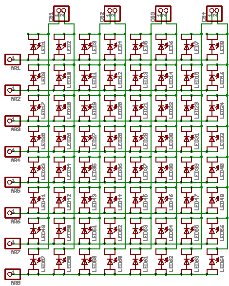
I designed the PCB to be a huge heatsink, with almost all the copper left intact on both sides. This matrix is wired as cathode column, anonde row. Each column is driven by a darlington on the daughterboard (more on this in my next post). Each row of the completed array will be driven by some beefy P-Channel MOSFETs. To facilitate the mounting of the daughterboard, which piggy-backs on the display board, I used some standard .100″ spaced pin headers, seen as CG1-4 and AR1-8 (column ground and anode row.)
The top, bottom and layout art are linked below to full-scale TIFF images, for making your own PCB. I also have a for a multi-layer image in the Paintshop Pro format, which has the top and bottom layers on a 100x150mm 300dpi layout, for making transparencies to use with small double sided pcb’s I have.
Here is a not-to-scale composite image of the layout and top+bottom sides for what I call the ‘display board’:

This is the schematic diagram of the LED array, showing the 64 indiv. LEDs and the connectors… linked to a larger version:

Here are TIFF format files of the various artwork layers at 300DPI:
Display Board PCB, Bottom Layer
Display Board PCB, Top Layer
Display Board Parts Layout
Control Board PCB, Bottom Layer
Control Board PCB, Top Layer
Control Board Parts Layout
** Note: Paintshop Pro Image Format!
Double Sided PCB Layout, one display, one control, plus some stuff for another project.
Please note, these designs, layouts, pictures, etc are not being released into the public domain. I reserve all rights as the creator and copyright holder. I do however permit the hobbiest to use these designs in their own not-for-profit projects as they see fit. I also permit redistribution of the design and images by hobbiests for the purposes of education and other not-for-profit uses. Please mention me and/or give a link back here if you post these on another website.
