It seems that my article on PCB Photolithography and Inkjet printers has surpassed the older articles on LED Sensors. It’s been a while since I’ve done anything with sensors. I still get quite a few e-mails about them, mostly folks asking specifically how to do something, or what the secret is. Honestly, I don’t know any more about them then what I’ve written. Most of my experiments took place on a breadboard, and were cobbled together from educated guesswork, trial and error, and a lot of reading. Perhaps I’ll revisit led sensors this summer – my PCB fabrication skills have really improved, and I can try making some ‘key pads’ which seems to be a popular request and application.
Jeff Han has started his own company selling his multi-touch technology. He never did reveal the ‘secrets’ to that impressive led matrix video which is so popular. From a business stand point, I can see protecting your IP assets, but led’s as sensors is old technology, I don’t think anyone today has a patent leg to stand on. In that light, perhaps if we all e-mail Jeff he’ll reveal his secrets to us.
Anyway, be sure to check out the ten most popular posts in the sidebar column. You can also check out the different project categories; each category has its own list of popular posts.
The single character LED sign I had been playing with now has a purpose! Shortly after discarding several ideas of having it as a serial display for PC/Server status, or hooking it up to the internet and a webcam, I came up with an actual useful purpose. The sign can be a clock! I have two ‘modes’ planned; traditional numbers and binary. All geeks love binary clocks, but most of us are lazy and would rather read regular ‘ol numbers.
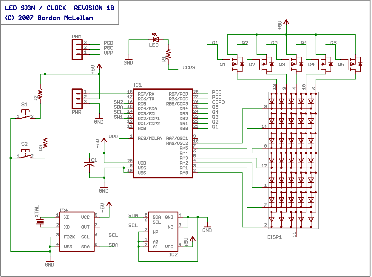
To facilitate the role as an clock, I had to redesign the circuit quite a bit. Two new ICs were added, allowing the LED Sign to keep time, and providing some much needed storage.
The first of the new ICs is a Real Time Clock. Because I’m cheap, I chose the M41T80 from ST Micro. It’s an inexpensive clock, similar to the Dallas DS1307 but lacking a few minor features. First, the clock has no power-on reset detection. It just starts up as soon as power is supplied. The Dall 1307 has a stop bit which gets set if the clock experiences a POR, so the firmware can test if the clock needs to be initialized or not. The T80 datasheet mentions some registers may get set to default values on power up, so I’ll have to read it a few more times to see if there is a way I can check for a POR. Second, the T80 has no support for a separate backup battery. Instead, ST recommends you place a diode in series with the clock, and use a large capacitor to provide backup power. Last, there is no automatic leap year / leap second correction, oh well!
The second IC is a 16 kilobit serial eeprom, similar to the Microchip 24C16, I chose one from Catalyst semiconductor due to lower costs. The eeprom is arranged as eight banks of 256 bytes each. The chip contains a 16 byte write-buffer, I’m not sure if it can cross a bank boundary or not, I’ll program my firmware assuming it can not. The eeprom will be storing character strings related to operation of the LED Sign as a clock, as well as user programmed messages and possibly simple graphics.
I’ve also added some micro switches for adjusting the clock and changing settings, also a 32.768kHz crystal was added to providing the timing source for the RTC.
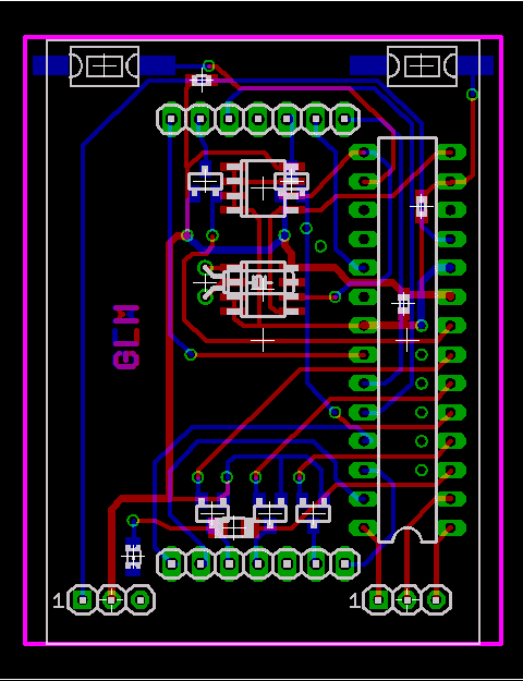
At this point, the layout of the printed circuit board has become pretty complex. I tried making one of these at home, but didn’t have the patience to exactly align the top and bottom layers of my press and peel sandwich. So, I decided to try a pcb prototyping house. There are a lot of board houses to choose from, many of which cost an arm and a leg. All of the domestic board houses are ruled out, I’m sure they do a fine job, but they cost too darn much. I settled on Spark Fun’s BatchPCB service. They’re not the cheapest board house out there, but their cost is fair. They include a lot of features most other board houses charge extra for, like double sided silkscreen and solder mask, 8 mil pitch and spacing, 20 mil holes, etc. I placed my order on the 6th, and had the PCBs by the 22nd. All the time in between, by mind set to wandering, and I made some POV toys. Once the pcbs showed up, I incurred another delay. Turns out I hadn’t ordered my RTC chips yet! So, another few days wait brought goodies from Mouser (man they are quick, and inexpensive!)
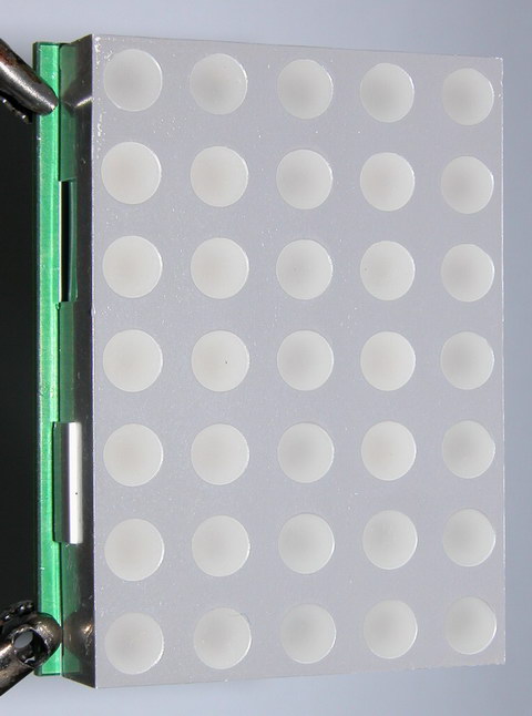
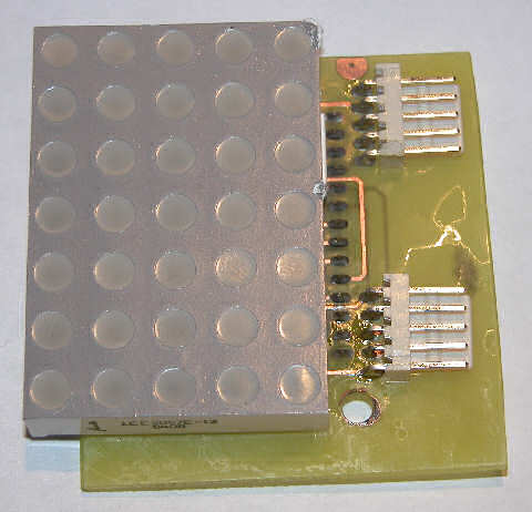
The boards from batchpcb look awesome. Nice bright green solder mask, tinned pads and holes, smooth clean edges. This is the ‘top’ side of my led sign. There are a few passives on this side, along with the two new ICs. This side is covered by the LED matrix once the board is fully assembled. Don’t mind the flux smeared everywhere – I did clean it off before soldering the matrix down.
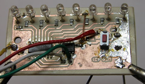
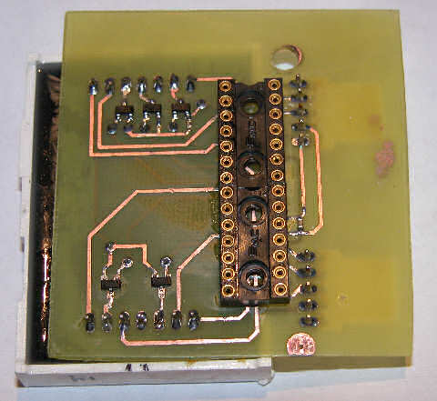
The bottom of the board contains the PIC processor, mosfet column drivers, a crystal for the clock and some microswitches. Pin headers for power and programming the microcontroller have also been installed. The module is a bit thick at this point, thanks to the socketed IC and the pin headers. On the finished version, I’ll solder the IC straight to the circuit board, and probably use wires instead of a header to supply power.
The firmware is in the early stages right now, so my next post on this subject will try to cover whatever features I’ve decided on. Right now I know I want a few things:
1. Scroll the time
2. Occasionally scroll the date
3. Occasionally scroll short messages, either randomly or programmaticlly
4. Support some sort of software brightness control
I’ve made some revisions to the design since I had these boards fabricated. One big oops I made was forgetting the pull-up resistors for the i2c bus! Luckily there’s plenty of room on the board, and both i2c lines ran near the Vcc rail. So a little quick scraping action to peel back the solder mask and presto, new lands for 0603 sides resistors. I’ve also added a diode and big capacitor for the RTC’s backup power.
I hope to work on the firmware more this week, so I should have more details about how the clock works next time!
I recently had the urge to create some “eye candy”; Thinking along the lines of my LED Sign (it’s not dead, just waiting on parts!), I chose to create a similar effect, using only a single line of leds, instead of a 5×7 array.
Persistence of Vision is some sort of effect, either psychological or biological in nature, that allows our eyes and brain to ‘see’ motion and patterns in a sequence of rapidly stills (hence a movie projection). This effect can be exploited using basic digital electronics to create a virtual LED sign, which the viewer will ‘see’ when the pov toy is put in motion.
Commercial POV toys are usually some sort of led matrix attached to a spinning contraption, and display either a fixed or scrolling message. Those are fine, but the technical aspects of motorizing the display make it beyond the scope of a simple project. Therefore, my project relies entirely on elbow grease – swing the wand and watch the messages appear.
Revision one of my POV toy is compact. It measures approximately 2.25″ length wise by 1.1″ width wise. The circuit consists of an inexpensive Microchip PIC 12F683 microcontroller, and a 74HC595 serial shift register. The display consists of eight 3mm leds, I chose blue for the first unit, but I’ll probably make a few more with different colors, I especially want to see green and amber – those leds don’t see a lot of action in the world of consumer electronics.
The circuit is very simple. A tiny microcontroller provides the brains, a simple and inexpensive shift register provides the brawn, and a switch and hall effect sensor provide some control. My first unit has no hall sensor, so power is controlled with the push button switch. When “off”, the pic is in a ultra-low power sleep state. Come to think of it, I could have put the shift register into a tri-state mode when “off”, but for now, it holds its gates at Vdd, which provides no bias across the leds, so there shouldn’t be much current going anywhere. The hall effect sensor will eventually control the power to the display, as well as provide some synchronization. Right now when swinging the wand, the message is legible in one direction, and backward in the next. I plan to try putting a small round magnet in a tube, and gluing it behind the hall sensor. When swung in one direction, the magnet will be forced over the sensor by g-force. When the wand is swung back, the magnet will be forced away from the sensor. This should let the microcontroller know not only to blank the leds during the ‘backward’ swing, but also how much time it has to render the entire message, speeding up the display for a quick swing, or slowing it for a long swing.
The circuit board is a single layer layout with two jumpers. I went with as many SMT components as I could afford, since I hate drilling holes in my home-made circuit boards. Power is currently provided by a 3.7 volt 1600mAh lithium ion cell.
I tried making some video of the unit in operation, but my camera wouldn’t play ball. Next weekend I may have more time to fiddle with photography and try to get some ‘action shots’.
Although version one has been a great success, and was easy, I was unsatisfied. The eye candy just isn’t sweet enough. Version two takes the flash factor up a notch, with RGB leds. I’m working on a ‘full color’ POV wand toy. Version 2.0 has been built, but it has some flaws – and is the subject of my next blog entry. Here is a video of “2.0” running a test pattern on its 24 led array.
This morning I hammered out a quick and dirty method to scroll a message on my single character LED sign. The scrolling is based around a few subroutines. A text message of 12 characters is passed to the scroll subroutine, along with the number of loops to make. The scrolling routine breaks the text message down into individual bytes, and loads up a static 60 byte message buffer based on data from the font table. Each “scroll” iteration causes the program to copy data from the message buffer into a 5 byte display buffer. The message buffer address is offset by one byte each iteration. Since one byte equals one column on the display, this action cause the display to appear to scroll. Another sub routine watches the address pointer, and wraps it around to the beginning when appropriate.
We’ve all seen the various sites where someone put a massive led sign online, and they let people abuse it. What I’ve managed to build is a “single character” led sign. I don’t know if I’ll be able to get my sign online, but I’ll take a stab at it.
After wasting a lot of time to convert a font table I borrowed from somewhere, my little sign finally had a built in character generator. It can generate any of the printable original ascii characters (dec 32 to 127), and display them on the matrix. Data feeds into the sign at 4800 baud (I think i mentioned 19200 earlier – way too fast), and is displayed on the matrix for a few seconds.
If the display sits idle for too long, a basic screen saver (screen waster?) kicks in, and does a simple animation. Any received characters replace the animation and reset the screen saver timeout.
Although exposed, I haven’t implemented the i2c interface yet. This pc board has some issues, and is too large. I don’t like the connectors sticking out to the side like that, so it’s back to the cad package to try and re-arrange things a bit. I think I will fork this design into two separate paths. One async serial (rs232), and one sync serial (i2c / spi). The sync version would be used as a display for other projects. The async version would be hooked up to a PC, and programmed with a simple message. Once detached, the display would just repeat the message over and over. One problem I ran into is storage. I had hoped to store text strings and the font table in eeprom, but the processor I chose, the 16f737 has no on-board eeprom. So instead, the font table is stored in the flash program space along with a few short text strings. The next revision(s) of the board will include a spot for a so8 ‘seeprom’ for extra storage.
I had purchased some huge (2″) 5×7 matrix a while ago, as part of my led sensor research. They’ve basically been banging around the lab since, getting pins bent and such. So this past weekend, I decided to put them to some other use. Their pin layout is sort of weird, it doesn’t match up with a breadboard at all (one of the reasons they never made it into the led research). So, I decided to make up some back-packs for them, or is it a carrier board? Anyway, the board features one 5×7 matrix, one pic 16f737, a few transistors and some data connectors. The board provides two means of serial communication; asynchronous rs232 at 19200 bps, or synchronous i2c at 100kbps. A second connector provides power and ICSP pins.
This project has no practical application as of yet. The main reason I made it was to improve on my double-sided pcb fab techniques. This time I found using point to point traces instead of a large “pour” made things work a lot smoother. I used the ‘sandwich’ method with press ‘n’ peel blue. Roughly 1.5 min per side.
One thing I had to keep in mind while doing this layout was accessibility to solder both sides, since I can’t through plate my own vias. So things had to be laid down in specific order. I soldered the vias first, using some cheap resistors with very fine leads as my conductors. The method involved sticking the resistor into the via, with just a bit poking out the other side, then bending the resistor 90 degrees and holding it to the board. Then a quick dab of solder onto each joint set them in place. Next, straighten out the resistor leads, and trim them off. Another quick few dabs with the soldering iron and each one was fully connected. Next came the smt parts. The switches were rather easy, but those blasted little 0603 capacitors always give me grief. I tin both pads, then apply a bit more flux as “glue”, then try to reheat one of the pads, to reflow the solder onto the part. It works great with 0805 and larger parts, but the little 0603 usually gets sucked onto the tip of the iron by the surface tension of the solder.
One hard choice I had to make was whether to solder the chip straight into the board, or use a socket. I opted for a socket, which meant a harder time soldering the “top” layer. Luckily, I was able to dig up some 14 pin machine pin sockets, and thanks to the machine pin itself, they stand proud of the board a little, just enough to sneak in with the soldering iron.
For whatever reason, I decided to solder the led display next, leaving the connectors for last. I partly wanted to see which side of the board the connectors would look better on… I think next revision, they’re going on the bottom. During assembly of the connectors, I nicked the display a couple times with the iron, oh well!
Right now, the display is flashing my initials. Oh, here is the schematic, nothing exciting really!
My apologies for not writing in some time. It’s certain not for lack of things to write about. I guess I’ve just been lazy lately. I don’t have anything specific to write about right now, but I wanted to make myself a list of things I need to document.
1) Art Light – Dec 2006
Decorative lighting for framed 3D art.
2) Mint Light – Dec 2006
Ultra small yet bright and versatile flashlight
3) LCD Adapter – Dec 2006 – Janurary 2007
Serial backpack for common parallel lcds
4) MintyBoost XL – Dec 2006 – Mar 2007
Twenty watt-hour portable power source
5) Cupric Chloride – Mar 2007
Experiments in alternative etching solutions
6) Toner Transfer – Mar 2007
Rethinking my bias against toner transfer
7) Stepper Motors – April 2007
Re-using an old paperweight.
There’s probably more I’m forgetting, hopefully I’ll amend this list when they spring to mind.
Usually my designs strive to create tiny boards, and I often obsess for days fine-tuning, shaving a fractions of an inch at a time. However, this design goal was get it done, get it working, then make it pretty.
I’ve been trying to build a switcher to provide a portable power source for PDA’s, cell-phones, etc. Not just enough to trickle charge said gizmo for hours, but to charge it as fast as possible, like the cradle or wall plug would do. This requires quite a bit of power. Packaging portable power is proving very tricky. There’s two main design goals I’m trying to meet. My primary goal the past week has been recharging the power-source, and the easiest way to do this is parallel cells. There’s oodles of charge management chips out there designed to handle charging of single lithium-ion cells (or parallel cells). The complexity knob gets turned WAY up once you start talking series cells. So rather than spin my wheels on this problem, I chose to move forward with goal number two. My secondary design goal is to get the power out. Putting the cells in series opens a wide door for easy to use switchmode converters and controllers. I’ve got a bin full of samples from all the big names, and I’m close to settling on a chip. First to prototype is the TPS5430 from Texas Instruments. This chip claims to have a three-amp switch on board, and it’s pretty easy to use. The switcher is internally compensated, eliminating an RC network often needed to compensate high frequency switchers. The 5430 comes in fixed voltage models, but I went with adjustable this time.
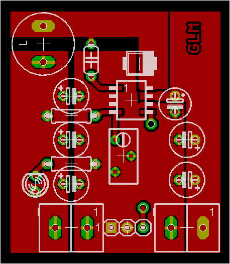
Using TI’s SwiftDesigner to generate a reference design, I drew that up in Eagle. Their reference design specified solid tantalum capacitors, which have properties that lend themselves well to switchmode applications. However, having priced 100+ uF tantalum caps, I’ve decided to use aluminum electrolytic instead. To offset some of the short-comings of aluminum caps, I have connected several in parallel. The main disadvantage is ESR, and wiring caps in parallel cuts the ESR dramatically.
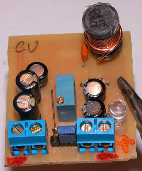
Loosely following TI’s reference layout, I came up with this design. I drew the design using the top layer, and ended up flipping it over when I assembled it. It doesn’t really make a big difference, just as long I remember to solder everything in a mirror image of what’s shown on the screen. For example, the screen shows the input stage on the right, but on the prototype, the input stage is on the left. The reference design called for a single 100uF solid tantalum capacitor rated at 25 volts (I spec’d 14v as VinMax). It also called for a 47uF tant as a bypass cap for the IC. So instead, I went with two 100uF 25v electrolytic caps and one 47uF 16v cap. I realize 16v is cutting it a bit close, but it’s all I could come up with, and this is only a first pass. The output stage called for a single 220uF 10v tant, instead, I drew room for three 100uF caps but only installed two for now. The chip needs a bootstrap cap to help it start-up with low input voltages. The datasheet called for 10nF, so thats what I used. The voltage divider is a 10k resistor coupled with a 10k pot. A resistor and LED were added to show “power on”. The three pin terminal at the bottom is tied to the enable line. Enable should float for normal operation and be pulled low for shutdown. I used a big ‘ol coil I had laying in the parts bin, it was labeled 22uH but the actual inductor is not marked. Looking at the size of the bobbin and heft of the wire, I’d say this inductor can handle some serious current. A three amp schottky diode completes this bit of kit.
With one set of fingers crossed, I hooked the switcher up to a wimpy 200mA 12v wall-wart, used for charging a screwdriver. To my relief the LED came on, nothing started smoking, and the ammeter read 10mA on the 10a scale (later I re-read 13.59mA on the 20mA scale). The datasheet claims 3-4mA of quiescent current, so the switcher is taking 10mA at 12v to supply 20mA at 5v. Although I haven’t done the algebra in the datasheet, comparing watts in to watts out puts the efficiency in the not-bad to pretty good range. (100mw / 120mw = 83%). Better still, when I connected my Dell PDA to the switcher, it was able to supply as much current as the Dell could ask for, without raising above ambient temperature. With a low internal battery, cpu set to 400mhz, external wifi card inserted, backlight full-on, the Dell peaked at 1.1 amps. I left it laying on the bench and watched a movie for a few hours. Coming back, the dell was completely charged, and the output had dropped to about 170mA.
My next goal will be to miniaturize this circuit as best I can, hopefully to fit it into an altoids tin which holds my lithium cells so very nicely.
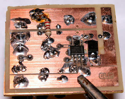
This is the second incarnation of my tps61040 based LED driver (here and here). As I wrote just a few posts ago, I’m trying out a new layout strategy to make my gizmos more breadboard friendly.
The 300 mil (thanks Dave) DIP16 package proves to be very small, so small I had trouble trimming it completely while depanelizing.
Another problem I ran into is a high voltage output cap. Seeing that this circuit generates upwards of 28 volts, the typical inexpensive ceramic or tantalum capacitors just don’t have the dielectric strength to work well. So, that leaves few options. Option one involves parallel smaller value high voltage caps. I ordered a bunch of 50v 1uF 0603 caps, so we’ll see how that goes. Second option is electrolytic. Sure I’ll incur some losses in the capacitor, dipping the efficiency a bit, but hey, it’s not a perfect world. I found some 10uf 4.3mm x 4mm caps that should do nicely. Third option is expensive ceramic … weighing in at $1 to $5 ea, these caps must be made of lunar rock. I have not ordered any of these, but I will look into harvesting some from dead / old electronics.
Notice the cute little inductor. That baby is 10uH, 1 amp, shielded and only 6mm square. Designed for high power applications, it has a generous saturation current, and rather low resistance. Even better, it’s only like 2mm tall, and to top it off is the cost; 59 cents each at quantity 10. In case you’re looking for an easy to use and flexible inductor, the digi-key catalog number is 587-1707-1-ND.
This time, in order to have a simple board layout, I chose to permanently enable the chip, so they’re be no dimming on this version. I’m not sure if the chip supports a hot load disconnect, I did manage to kill my earlier prototype somehow, one of the output leads broke off the pcb while I was holding it, in a dark room. After repairing the damage, I only get a very low output. Perhaps my capacitor or diode was fried.
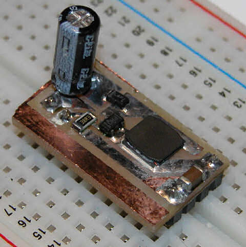
Here are the breadboard compatible pins. The three pins are the output area, with the one inboard pin being the led sink, where the current sensing resistor is attached. This layout required two ground pins, and an external jumper to connect them. I’ll remedy that in the next iteration.
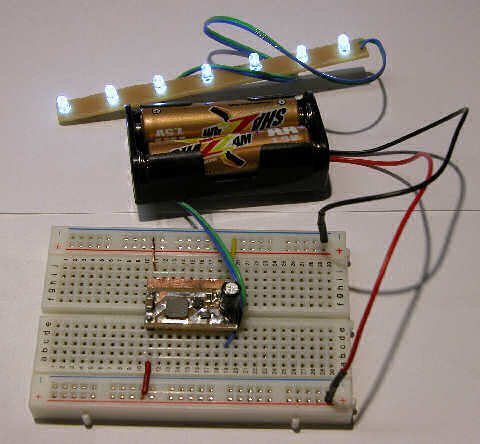
This is the little critter doing it’s thing. Do you like that battery brand? SHAZZAM – it just screams power. I bought a BUNCH of these at a traveling tool sale show, 99 cents for 16. They’re not half bad for light loads, this little switcher sucks ’em dry in a mater of hours however!
Seeing as how my project log is more than a year old now, it is overdue for a new coat of paint.
Presenting “I feel dirty 1.0 by The studio ST team”. I’m not sure about the name, but I do like the little bit of color, but still mostly plain white. Hey, I like plain, but a friend thought my original choices of all white (like Water 1.1) were just too plain, so here we are.
I think I’ve copied all my mods from the old theme, if anyone happened to be viewing the instance I was making changes, well, it probably looked a little funky.