A few ideas, but still too hot.

I’ve been rolling a few idears around in the brain box, in preperation for re-opening the lab, since the summer heat is on its way out.

Number 1: Eclipse mints based usb charger / battery. I like the esclipse tin better than altoids gum, since its more square and only has a small opening via a hinged lid at one end. It should hold two lithium ion cells and a small PCB quite nicely. My plan is to make the gizmo with a small switch (or automatic possibly), so it can both charge/operate USB devices. or recharge off a USB host.

Number 2: Ice breakers mints based palm light / flashlight. Take a metal ice breakers mint tin, slap in some lithium cells, a USB re-charging circuit, add a 6 watt luxeon K2 and presto… nice and bright palm-sized flashlight. I also thought about adding a USB capabile microcontroller, and having the device show up as an HID gizmo in windows … perhaps allow programming of different brightness levels, check battery, etc.

Number 3: USB controlled Luxeon 1 based keyboard light. Using some semi rigid tubing of some sorts, and a not-yet-found small metal enclosure, create a usb HID based keyboard light for using on my laptop.

Thats all I got for now – till next time!

RS232 Utilitarian Project

If necessity is the mother of invention, being cheap must be like a step-father or uncle or something?

I needed some level shifters / line drivers that I could easily use on the breadboard for microcontroller projects. Rather than give some other entrepreneur $10 for their version, I made my own.

MAX232 rs232 line driver level shifter

Nothing particularly special here, aside from the cool factor added by the two LEDs which light on RX/TX events. The chip is a standard MAX232 clone, and I’ve got five 1uF ceramic caps mounted on the back side. The leds are driven by some SOT-23 transistors. To make things simple, I stuck the pin header through the board the “wrong way” and forced the pins almost all the way through their plastic spacer / retainer. This way the unit plugs right into the breadboard, and lays there real nice, even with a heavy serial cable attached.

MAX232 rs232 line driver level shifter

So far so good, it works well with my bootloader at 115kbps, so I figure that’s good enough!

EDIT: Eagle SCH and BRD files available here (7-zip format).

DIY PCB Fab Pictures

As sort of a follow-up to my Inket Photolithography article, I have some more pictures of the process, from start to finish.

paint shop pro pcb panelize

Using paintshop pro, I take individual PCB layouts and combine them into a composite panel, which is the exact size of the PCB I’m going to expose. Often I’ll repeat the same design a few times, in case there’s some glitch in one of them, or the board is damaged during the depanelizing process. I like to start with a black background for the panel, to mask out any unused sections of copper… this helps cut etching times and helps save the etchant life.

The inkjet transparency comes with a sheet of white paper attached, to protect the transparency and give the printer something extra to grab onto with the feed rolls. It takes about 30 min for the ink to fully dry.

This is my darkroom which also doubles as my house’s furance room. The exposure system is two cheap-o under cabinet lights, with “daylight” bulbs loaded in them. The timing is completely manual and is just an extension cord I unplug when time’s up.

After exposure, the PCB takes a bath in a sodium hydroxide solution to develop the resist layer. Within a few minutes resist that was softened from exposure to light is dissolved away. I rinse the board in hot water (per manuf. spec) to check for complete removal of the resist – sometimes a thin film remains and another dip in developer is required. After all is well, a rinse in cold water sets the resist and halts the developing process.

pcb inket transparency

Here is the transparency used to expose the photosenstive printed circuit board. It is actually laying on top of the board which as already been etched.

diy pcb fabrication

The resist is a blue color when it’s “active” and turns green after it has cured, and is no longer photosensitive.

diy pcb fab protective equipment

Protecting eyes, ears and lungs is a very important step.

diy pcb fab drill dremel carbide

My drilling station is a basic dremel mototool (single speed) mounted in a drill mini-press. I have two 20 watt halogen lamps to illuminate the panel, one is a flood/fill light, the other a tight focus spot right on the cutting head. Using expensive aluminum titanium oxide coated solid carbide drill bits (designed for drilling fiberglass and non ferrous metals like titanium), the dremel easily pierces the board, spinning at 35000 RPM.

diy pcb fab drilling

Lots of holes!

diy pcb fab protective equipment

Make sure your safety gear is still on!

diy pcb fab depanelize

A visit to the impromptu depanelizing saw aka a Skill Jigsaw turned upside down and secured in a bench vice. With the blade installed backward, the foot of the saw provides a nice table for resting the panel on. This arrangment will gladly take a finger or at least mess you up, so make sure you have no distractions and always know where your fingers are while the blade is moving. Sometimes you’ll end up with pieces that are pretty small, but it’s not worth the risk of serious injury trying to do them on the saw… scoring both sides of the pcb with a drywall knife should let them snap cleanly… also I’ve heard large sheer-type paper cutters work.

diy pcb fab depanelized

The end result, a pile of little PCBs.

Sometimes the saw doesn’t leave the cleanest edge or your line is a bit wavey – a visit to mr belt-sander will clean things up nicely.

editors note: some of the pictures for this article didn’t come out as well as I had hoped, or have yet to be taken, so the [image missing] tag is a place holder to remind me to reshoot.

TPS61040 Constant Current Driver

I’m already up past my bedtime, so just a few pictures for now. Write-up coming soon!

Specs: Input 2v to 6v DC … Output constant current 50mA up to 28v DC
Efficiency: Initial measurements, somewhere around 75%
Chip Texas Instruments TPS61040

tps61040 boost converter constant current led driver
size comparison, american quarter dollar piece


circuit detail – design is one-sided PCB with two through-hole jumper wires and the diode, everything else is smt


twin 1uF tantalum capacitors … the output capacitor I had originally selected was limited to 16v, so this was the best I could come up with on a Sunday. Note the top of the coil is missing – these things are fragile!

PCB Photolithography and Inkjet Printers

I may be easily amused, but I’m not easily impressed.

Everything I have read about pcb prototyping using photolithography claims I needed to use a laser printer and some sort of transparent or translucent medium. Armed with this knowledge, I used acetate, or overhead projector transparencies. The film claims to be designed for laser printers and copiers, but it still distorts some when printed on. Anyway, the problem with my laser printer is toner pin-holes. For whatever reason, the output would have these little holes everywhere, and these little holes would swiss-cheese my traces and ground plane pours. This forced me to use thick traces, which would still get swiss cheesed, but generally retained enough composure to be electrically conductive. The pin hole problem seems to be getting worse … the last test I performed on my printer as an exposure test of varying width lines and different sized holes and pay layouts. In general, the performance was pretty bad and was not acceptable for more advanced designed I wanted to make, involving very small SMT components.

So, I tried printing the same exposure test, on paper, to my inkjet printer. The results were stunning. The lines were sharper, the holes clearer, the pads better defined. What a difference it makes going from a 600 dpi laser to a 4800(?) dpi inkjet. So, I felt it worth the risk, and decided to run my exposure test with the inkjet. Using some inkjet transparencies (they’re kinda coated with some type of fiber?), I printed my patterns. I exposed my board, and then developed it… the results were WOW! Of course, I messed up a few things with this first run, mostly I let the light cook for too long. So in the best un-scientific manner possible, I changed a bunch of variables at the same time, and tried another pass.

photolithography inkjet pcb

That is the result! … Please ignore the greasy thumbprint on the left side of the board – that was acquired after etching, and has no effect on anything aside from mild embarrassment on my part. My setup was fairly simple. I printed my design at best quality, monochrome mode onto a transparency. Next, in my darkroom that doubles as a furnace room, I laid down my PCB, emulsion up, then the transparency, then a sheet of 1/4″ plate glass. About 4″ above that, I have two 15 watt under cabinet lights, each loaded with a GE Daylight bulb. The lights are connected to an extension cord, so I can turn them on and off together. After making sure everything is lined up, I start my stopwatch and plug in the lights. After letting it cook for eight minutes, I turned off the lights and slid the pcb into a waiting bath of developer. The developer had been sitting for about a day, so it was a little slow. I left the board sit for about 2 min, before turning on the room lights. As the emulsion started to dissolve, I could see the results were good, real good! With the room lights on, I stirred the developer and lightly brushed the pcb using a foam brush (as recommended by the manuf.) My image grew sharper and sharper.

After I was sure all the emulsion that needed to be gone was gone, I rinsed the board and slid it into a waiting bath of ferric chloride etchant. A few min later, I pulled the pcb out, to make sure all the copper had turned pink. If the copper is not pink, it means some emulsion remains, and its time for another trip to the developer. Fortunately all the copper was pink, no problems here. I let the pcb soak for about 30 min while I had some lunch. After lunch, and without washing my hands i might add, I extracted the PCB from the etchant and rinsed it off. The results are excellent.

So, no longer will I shy away from tiny SMTs, since I can now lay down traces as thin as 8 mils without issue (determined by the earlier exposure test). Granted there were three flaws I had to fix on this board, I suspect they were caused by either dust on the transparency or those fibers that are embedded in the plastic. A quick touch-up with the sharpie solved them without a hitch.

Next stop, de-panelize with the PCB “suicide” saw.

pcb saw depanelize

Audio Matrix Switch

I’ve had some down time project wise lately, most of my SMPS research is on hold, since I need to order even more parts (namely diodes and switches)… so, I’ve taken the time to draw.

One of my ‘back burner’ projects is a whole-house audio distribution system. So, this past week or so, I set out to design the heart of the system, a matrix switch. Originally I had tried to go “too big”, designing a system with four inputs and eight outputs. However, routing the signal lines and control lines was too much of a challenge, even using a two layer board. So, scaling things back, I wound up with a 4×4 matrix that was barely manageable.

audio matrix switch 4x4 74hc4052 74hc595 schematic

There is the schematic for the latest ‘stable’ version. I call it a stable version, because it passes all of the DRC tests and all the nets are routed. I have another version in design, which adds ESD protection to the external audio connections in the form of high speed schottky diodes which will clip any voltage coming in that rises above or falls below Vcc and Vee.

Control will be provided by either a serial / parallel connection to the audio server PC, or from a “controller board” powered by a microcontroller. I haven’t really figured out how complex I want to make the interface yet. Control of the switch itself is fairly straight forward. Two 74HC595 latching registers are daisy chained together, forming a sixteen bit register. This register is used to provide the eight bits which tell the multiplexers which connections to make. Each multiplexer has a two bit interface, A and B, which selects one of the four IO channels to be connected to the COM channel. I selected the 4052 multiplexer which is internally divided into two sets of four channels each, ideal for stereo I thought. So the first eight bits of my 595 register are connected to the eight control lines on the 4052’s. Second, to provide a “hardware mute” or “output enable” feature, another four bits of my 595 register are connected to the /Inhibit (enable) control lines on the 4052’s. This allows the output of each 4052 to be electrically disconnected from all the sources. The final four bits of the register are used to power four “general purpose outputs”, perhaps to control relays, external indicators, whatever. The control lines connecting to the GPO header have inline resistors, to limit current draw to a safe level, so not to damage the 595 in the event of a short or connection to an unsuitable load. The four bits connected to the inhibit lines are also connected to four LEDs, so I can see which zones are active.

The 74HC4052 is an “analog” multiplexer, in that it allows voltages other than digital 1’s and 0’s to pass through. It is also a bidirectional multiplexer, allowing current to flow in either direction. This allows the multiplexer to handle the “AC” nature of an audio signal. In order to allow a true bipolar sine wave to pass, the 4052 requires a dual rail voltage supply. For simplicity, I will be using a five volt supply with positive and negative outputs.

two layer pcb layout audio matrix switch

Here is the ‘bare’ pcb layout, without the top and bottom pours rendered. This is a composite, showing both the top layer and bottom layer at the same time. It’s easier to follow the traces this way I think.

two layer pcb layout audio matrix switch

Adding in the ground planes or copper pours, it makes the board look mostly purple. I tried to maximize the size of the pours, to help minimize any interference or crosstalk. Although, at such low frequencies, I don’t really expect much trouble.

pcb parts layout silkscreen audio matrix switch

Finally, the board with just the silkscreen or layout layer selected. This again, is a composite, showing parts on both the top and bottom of the board, which makes it look like some of the parts are overlapped.

There is a lot more to come on this subject, but it will be a while. Overall, this was just a fun project to draw, and hopefully one day it will actually get fabricated. I need to figure out how complex I want the interface to be, and what options I have for interfacing with the audio server.

TPS61040

Most of the applications for LEDs I’ve run into require a lower than supply bias voltage for the LEDs. This situation is fairly easy to deal with, you can use a current limiting resistor, a linear regulator, or in high power applications, a step-down or buck converter.

However, occasionally, it may be beneficial to have a rather high LED bias voltage, even with a low supply voltage. For example, in small battery powered applications, rather than run your LEDs in largely parallel configurations (which has many drawbacks), you can string the LEDs together in a large series string, and then parallel those strings if need be.

Enter the TPS61040 from Texas Instruments. The TPS61040 is an integerated high efficiency step-up or boost converter. It is a integerated converter rather than a controller, because it contains both the power switch and the feedback circuitry. This means a very simple design is all that’s required to make it work – and in my opinion, the smaller the part count, the better.

tps61040 step-up boost converter smps led driver

There is my schematic, which provides for a variable voltage constant current “LED Driver”. LED current is programmed by resistors R1 and R2, which are connected in parallel. Inductor L1 is a small 10uH inductor, and D1 is a ‘standard’ schottky diode. C1 and C2 are low ESR ceramic capacitors, with an X7R rated dielectric. The chip itself, IC1 is an amazingly small SOT23-5 package surface mount IC. The rest of the components are also surface mount, both for space savings and laziness, as I hate drilling holes. I was out of SMT schottky diodes at the time I drew this, so D1 is a 2.8mm by 7mm DO41-7 package. C1 can be a 10 or 16 volt cap, C2 should be rated at the output voltage plus a safety factor (for dealing with ripple). L1 should be sized to handle the current demands of the circuit – I just went with 1.6 amps since it was cheap.

tps61040 pcb layout artwork

The layout is about 20mm square. My intended application is for lights inside a “shadowbox” style picture frame. I want a small string of white LEDs powered by some cheap AA batteries. I’m out of PCB developer right now, so no PCB fab this weekend. Once I get some more in, I’ll share the finished product with everyone, as well as some pictures of my cheezy art project.

If anyone should want full resolution layout or pcb artwork, just hit the contact justdiy button, over in the right hand sidebar.

Touch Sensing Building Blocks I

The “core” building-block I mentioned in my last post is nearing completion, at least, the software.

I have my microcontroller handling “switch emulation” tasks. It can emulate either group of momentary switches or a group of toggle switches. Response time is real good in a dimly lit room, and it works decently well even with the overhead fluorescents turned on.

Right now I’m working on a basic keypad PCB I can throw together, for a ‘proof of concept’ prototype. The first keypads will likely only support 6 keys, and I’ll build from there. Six keys requires twelve LEDs, six of them need direct and discrete anode and cathode connection to the microcontroller. The other six LEDs are providing bias light for the sensors to “see”.

I should have a video up tomorrow of the breadboard in action, and hopefully some pcb’s by next weekend.

LEDs As Sensors: Revisted

Thanks to the folks at Make: and Hack A Day, my research into the area of using LEDs as sensors has been receiving a lot of attention. With this attention comes questions. I like receiving questions. Only thing I don’t like about answering questions in the e-mail is the knowledge is locked up. Sure I could repost the e-mails, but it is sometimes difficult to follow the context after the thought train has left the station. With my rekindled interest, I wanted to take a short moment and summarize a few things.

These are just my opinions – and I welcome debate and feedback on them – I especially welcome anyone to be challenged by them enough to prove me wrong. LEDs as Sensors offer at least two avenues of usefulness; communications and interface. I haven’t dipped even a toe into the communications side of the pool – all my work has been on interface.

These are the applications I feel LED Sensors are a poor fit to replace:
#1 – The touchpad on your notebook. Seriously, no one but a geek would enjoy having 128 or more bright LEDs glowing continuously to replace the little capacitive discharge pad that is used 95% of the time today.

#2 – The keys on your keyboard. LED sensors are pretty slow, even a modest typist would be hindered by the response time.

#3 – Any application that needs to work outdoors. LEDs and the Sun do not get along.

These are the application I feel LED Sensors may work well in:
#1 – Keypads and interactive displays used for Art and Music. These applications fit the ostentatious nature of the interface, where the controls are as much a work of art as a functional device.

Yep, that is it… that is the only application I think LED Sensors offer any strength in.
Here is an example – Musician / DJ sound effects tablet:

Imagine a thin tablet like device, glowing brightly with powerful LEDs in an otherwise darkened club / dance hall / etc. The tablet accepts an ordinary 8×11 sheet of transparency film. Printed on the film are the names of pre-programmed effects / samples /whatever. Under the film, evenly spaced trios of LEDs are used to detect the presence of a reflective object. The tablet connects into the rest of your system using regular MIDI or whatever other interface one can think of. This tablet is no different than boxes hobbyists and musicians have been building or buying for years, except, the mechanical switches have been replaced with eye catching LEDs.

Here are a few other questions that have been raised:

Q: Do I have to use red LEDs?
A: No, technically any LED color works. Red is the cheapest and that is what I use. Along with yellow, red is almost the most sensitive.

Q: I tried IR LEDs and they seem very sensitive, why not use those?
A: The point of using LEDs as Sensors is to have an ostentatious interface. It’s not going to be very showy if the light is invisible. If you want to use infrared LEDs, use one emitter and one photodiode / phototransistor – it is a LOT easier.

Q: Does this work with organic / flexible LED displays?
A: I have no idea. Those displays are largely theoretical and prototypical in nature – maybe in five years when I can buy one for a few dollars, I’ll experiment with it. The organic compounds used to manufacturer these displays also have big problems with humidity and overall short lifespan – neither are very positive traits.

Q: Can you send me your ASM code for such and such?
A: No, no I can’t. I do not have any ASM code – I do not know how to program in assembler. I have code written in Proton Basic, which I will happily share.

Q: I want to get started with microcontrollers?!
A: Excellent – I’m not going to help you. There is a huge learning curve involved – a lot of it can be skipped by spending money (on proton basic). Check out www.sparkfun.com and www.crownhill.co.uk for good microcontroller stuff. Check out google.com for tons of info on learning microcontrollers.

Q: What microcontroller do you recommend?
A: I like the new PIC16F690 family from Microchip. It is a small inexpensive package that offers many features only found on larger processors (like dedicated i2c hardware). It also sports at least 10 ADC ports.

——

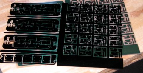
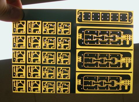
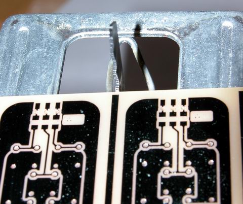
In closing, I would also like to share some basic info on what I’m working on at the moment. My current project is to get a stand alone system worked out for emulating mechanical switches. I consider this a valuable “core” building block behind the technology. I have momentary switches partly working, after that, a toggle switch shouldn’t be much harder. As a future goal, I would like to get “cores” built to emulate sliders and knobs. Those three elements should cover a great deal of the artistic / musical needs that I feel this technology is well suited for.

Thank you for visiting and I welcome your comments. My gmail is gordonthree – feel free to contact me about anything.

Water Filter Controller

The old adage “measure twice, cut once” has a realitve in the field of electronics engineering; “measure twice, design once” … ok, well maybe that’s a bit corny but anyway.

Turns out the controller I designed for my water filter is pretty much useles. My filter’s pump is not the 12vdc that I imagined it to be, instead, it is 24vac. So the two smt mosfets which I soldered to my pcb with generous amounts of solder, are not capable of switching AC. Worse, I had planned to power the controller itself off the psu for the pump, so the 7805 vreg I’m using will not appericate AC on its input terminals either.

I plan to salvage this situation however… using relays, either mechanical or electronic, as well as a separate power supply. So, I will use a ~12 volt unregulated supply to power a pair of mechanical relays, one for the pump, one for the valve, which in turn will be switched by the mosfets. Or, I can desolder / destroy / jumper over the mosfets, and run a +5v control signal to my outputs, for control of a solid state relay.

I need to price out the cost of mechanical vs solid state …. probably solid state will win, I think I can build a triac based ssr for under $2.